Shenzhen Vatop Semicon Tech Co.,LTD

139 2576 7787

Vatop Semicon

Shenzhen Vatop Semicon Tech Co., Ltd., founded in Nov 2019, has the strong capacity for product research and development in the semiconductor field. The technology driven company has the most complete and professional development team for Die Bond & Wire Bond& detection technology in China. We wish to deliver the highest value to the market through the products and motivate the semiconductor technology's upgrading in China with intelligent detection technology.
The founded team members have at least 20 years of work experience in Mechanical, Optical, Algorithm and several fields in foreign leading semiconductor enterprises. Members of the team have obtained doctoral and master's degrees from the University of Hong Kong, The National University of Singapore, Harbin Institute of Technology, Beihang University, Sichuan University and other world-class universities. Almost 60% of the employees in Vatop Semicon have the experience working in semiconductor related industry. That form the basis of the development of the enterprise.
At present, Vatop Semicon has been obtained tens of millions of financing that leads by ShenZhen Government Guidance Fund, dozens of related patents have been applied for. The main products includes, Die Bond & Wire Bond Automated Optical Inspection Machines, Wafer Automated Optical Inspection Machines, etc. Based on the core detection algorithm and optical module which are under independent intellectual property rights, Vatop Semicon could achieve fast response to customers' needs and provide customized services.

core advantages

  • Expertise

    Capacity for Product Development

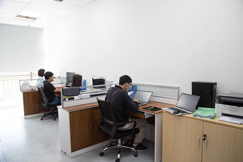
    Core team members have at least 20 years of experience in the semiconductor industry
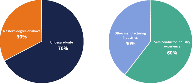
    90% of the members have a bachelor's degree or above
    60% of the members have experience in the semiconductor industry
    30% of the members have experience working overseas

  • Focus

    Focus on Inspection Equipment in Semiconductor Field(AOI)

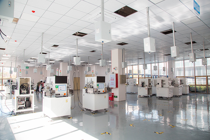
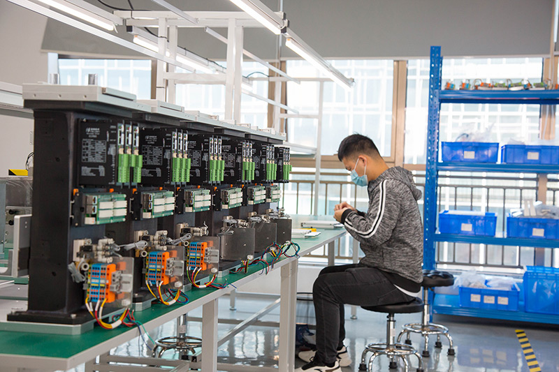
    Wafer defects in wafer field
    Die bond defects in IC field
    ire defects in IGBT field
    Products defects in LED field

  • Reliability

    Independent Intellectual Property Rights for Core Technology

    Self developed vision algorithm and opitcal module
    More intelligent with the use of deep learning
    Fast response and provide customized services
    Focus on innovation and sustainable development

Our culture

  • Vision

    Being the leading solution provider in semiconductor detection industry

  • Mission

    Focusing on customer demands,hasten the evolution of technology innovations,delivering the maximum value to the customer and market.

  • Values

    Integrity and responsibility,teamwork-based creation process & win-win cooperation,innovation focus,continuous improvement

development path

R & D talent composition

social responsibility

We do believe that a successful enterprise must be responsible and contribute to the society and community. We are committed to ensure the protection and esteem of our employee, the consistency of business and ethical standards, the safety and comfort of work environment, and the fast response to the needs from society.